2. Interfaces#
Jaguar provides a wide variety of interfaces.
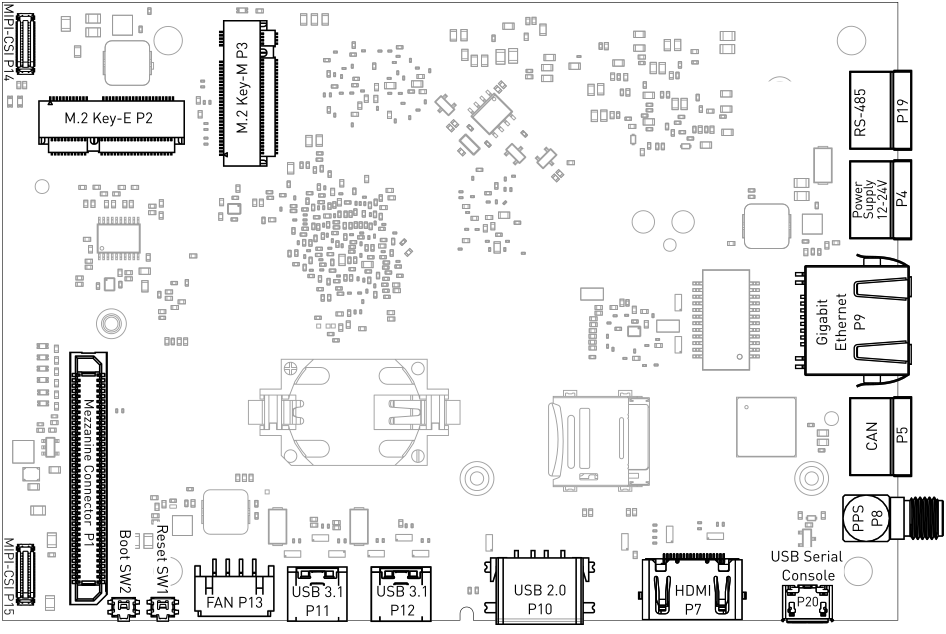
Fig. 2.1 Jaguar interfaces overview#
2.1. Power Supply#
In order to power the board, connect the appropriate cable to the highlighted connector shown in the figure below. The Jaguar power supply voltage is 12-24V.
Note
Be careful when connecting the power cable since all three terminal block connectors are of the same type.
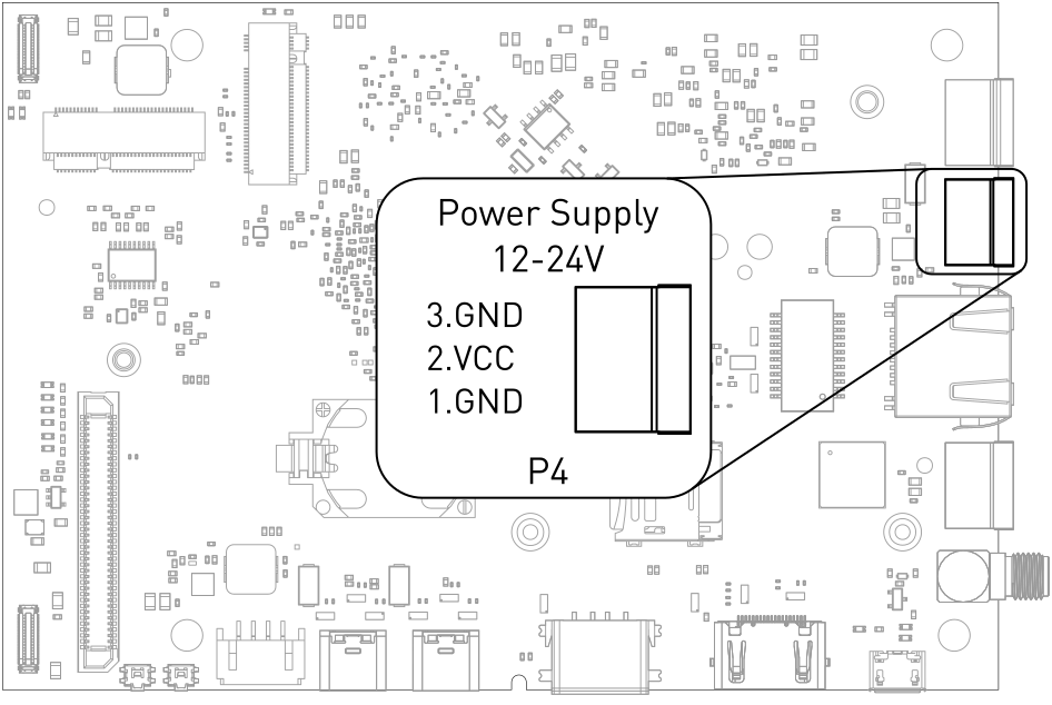
Fig. 2.2 Power connector#
Manufacturer |
Partnumber |
Description |
|---|---|---|
Würth |
Vertical |
|
Würth |
Horizontal with hook on wire Side |
|
Würth |
Horizontal with hook on back Side |
|
Würth |
Screwless Plug Vertical Entry Low Profile |
2.2. USB Serial Console#
Jaguar contains an on-board Silicon Labs CP2102N USB-serial converter. Connect a Micro-USB cable to the Micro-USB as highlighted below:
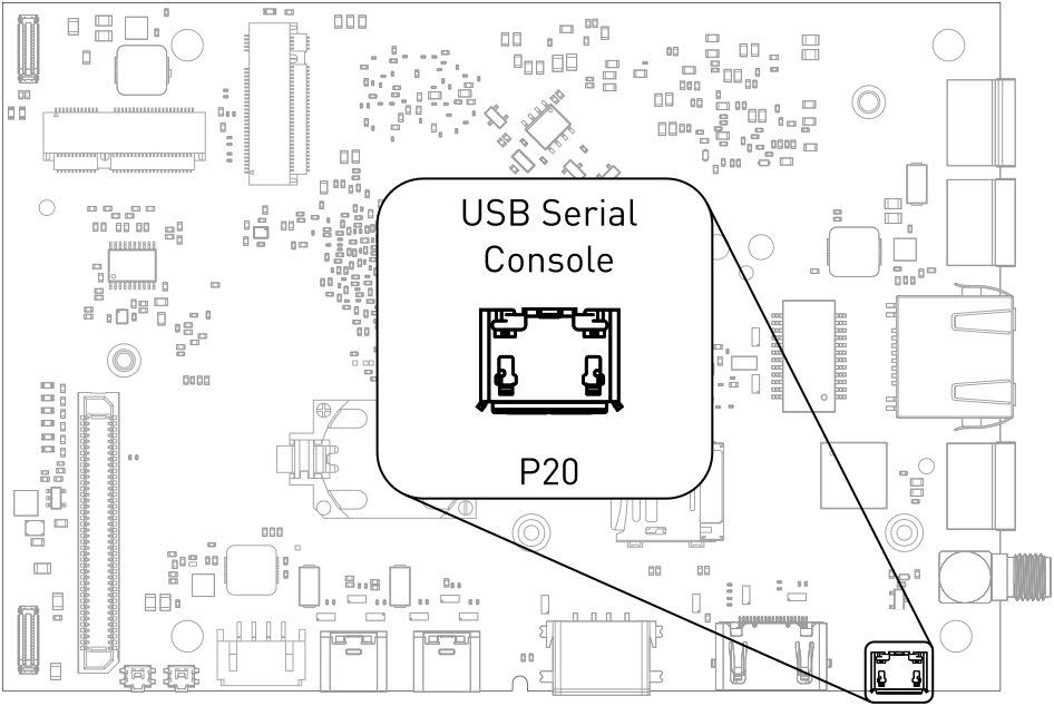
Fig. 2.3 USB UART#
For macOS and Windows, drivers are available from Silicon Labs: https://www.silabs.com/products/development-tools/software/usb-to-uart-bridge-vcp-drivers
A terminal emulation program is required to access the serial console.
Operation System |
Terminal Emulator |
URL |
Example Commandline |
|---|---|---|---|
Microsoft Windows |
PuTTY |
||
MobaXterm |
|||
Tera Term |
|||
macOS |
cu |
|
|
Linux |
picocom |
|
|
minicom |
|
||
GNU Screen |
|
Note
Make sure to disable software flow-control (XON/XOFF). Otherwise, serial input may not be recognized.
After system boot-up with the Jaguar Debian development image, the login console appears on the terminal:
jaguar login:
You can log with one of the following credentials:
Username |
Password |
|---|---|
root |
root |
user |
123123 |
2.3. Buttons#
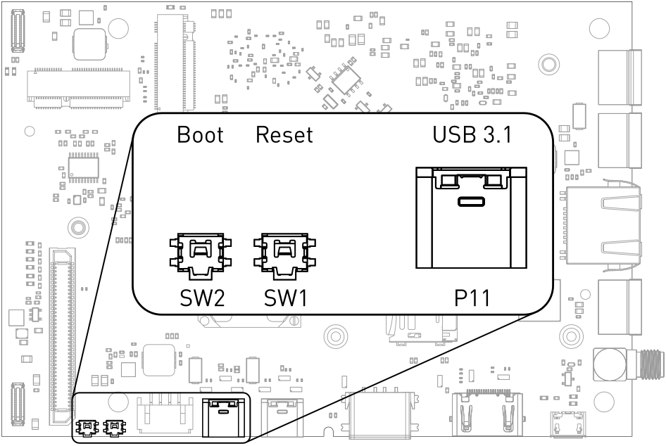
Fig. 2.4 Buttons and Download USB Type-C port#
The control buttons provide the following functionality:
Resettriggers a board reset.BOOT SWforces alternate boot sequence.
2.3.1. Boot Order#
The used boot order of the Jaguar board depends on the state of the BOOT SW
switch.
Default |
|
|
|---|---|---|
1 |
eMMC storage |
SD card |
2 |
SD card |
USB loader |
3 |
USB loader |
If no bootloader is found on any storage device, Jaguar will go into USB loader
mode, showing up as a USB device with VID:PID 2207:350b on the USB port P11
marked Download.
Once booted into Linux, presses on the BOOT SW button will trigger a
KEY_VENDOR input event on the /dev/input/by-path/platform-adc-keys-event
input device:
$ evtest /dev/input/by-path/platform-adc-keys-event
Input driver version is 1.0.1
Input device ID: bus 0x19 vendor 0x1 product 0x1 version 0x100
Input device name: "adc-keys"
Supported events:
  Event type 0 (EV_SYN)
  Event type 1 (EV_KEY)
    Event code 360 (KEY_VENDOR)
Properties:
Testing ... (interrupt to exit)
Event: time 1695722632.280609, type 1 (EV_KEY), code 360 (KEY_VENDOR), value 1
Event: time 1695722632.280609, -------------- SYN_REPORT ------------
Event: time 1695722632.383952, type 1 (EV_KEY), code 360 (KEY_VENDOR), value 0
Event: time 1695722632.383952, -------------- SYN_REPORT ------------
2.4. FAN#
A PWM controlled fan with tacho signal can be connected. The supply voltage can be selected by changing a 0-Ohm resistor, the default supply is 12 V.
Resistor |
Fan supply |
|---|---|
R314 |
Main supply voltage |
R315 |
12 V |
R316 |
5 V |
Manufacturer |
Partnumber |
|---|---|
JST |
PHR-4 |
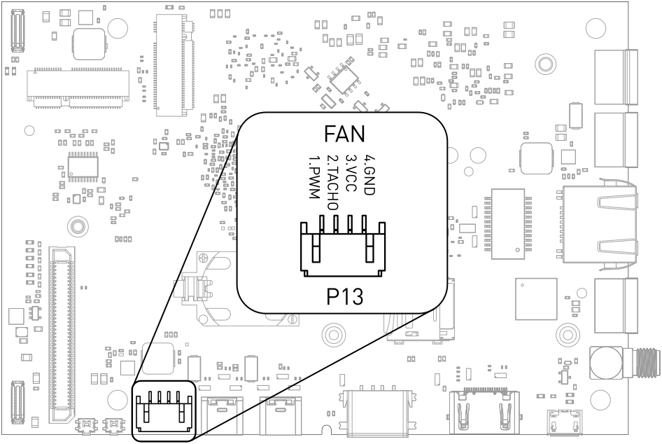
Fig. 2.5 FAN connection#
2.5. CAN#
Jaguar supports up to three CAN busses. CAN0 has an on-board transceiver and supports up to 1 MBaud data rate. CAN1 and CAN2 are available on the Mezzanine connector and require a transceiver on the Mezzanine board.
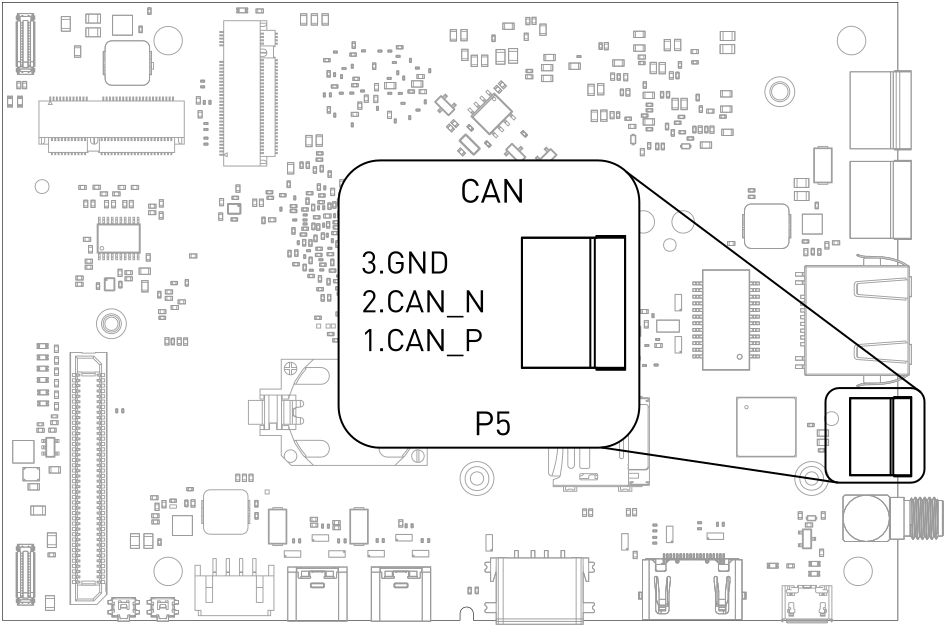
Fig. 2.6 CAN connector#
Manufacturer |
Partnumber |
Description |
|---|---|---|
Würth |
Vertical |
|
Würth |
Horizontal with hook on wire Side |
|
Würth |
Horizontal with hook on back Side |
|
Würth |
Screwless Plug Vertical Entry Low Profile |
2.6. RS-485#
Jaguar supports half-duplex RS-485.
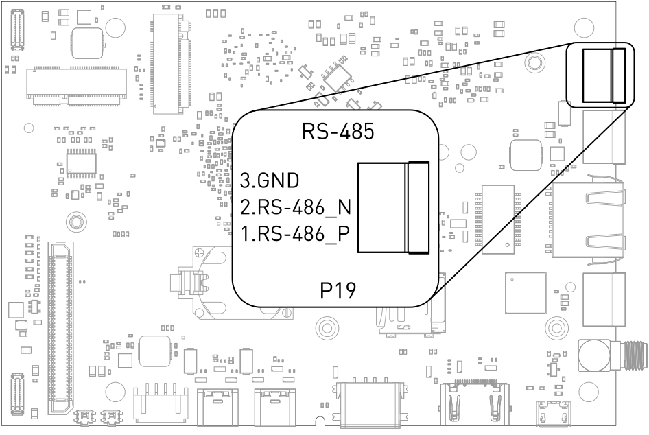
Fig. 2.7 RS-485 connector#
Manufacturer |
Partnumber |
Description |
|---|---|---|
Würth |
Vertical |
|
Würth |
Horizontal with hook on wire Side |
|
Würth |
Horizontal with hook on back Side |
|
Würth |
Screwless Plug Vertical Entry Low Profile |
2.7. Battery#
A CR2032 coin cell can be used to supply the on-board real-time-clock. The coin cell is only used when Jaguar is not supplied power from an external source.
2.8. Mezzanine Connector#
Jaguar has an 80-pin connector for extensions board. Most pins have multiple functions that can be selected via software configuration. See Table 2.10 Mezzanine multiplex functions.
Manufacturer |
Partnumber |
Description |
|---|---|---|
Hirose |
2mm height plug |
|
Hirose |
5mm height plug |
Pin |
Function |
Pin |
Function |
|---|---|---|---|
1 |
CP2102_POWER_EN |
41 |
GND |
2 |
CAM0_STROBE |
42 |
GPIO3_C0 |
3 |
ADC_IN2 |
43 |
CAM2_CLK0_P |
4 |
CAM1_STROBE |
44 |
GPIO3_C1 |
5 |
WDTRIG# |
45 |
CAM2_CLK0_N |
6 |
I2C1_SCL |
46 |
GPIO3_C2 |
7 |
GND |
47 |
GND |
8 |
I2C1_SDA |
48 |
GPIO3_C3 |
9 |
CAM3_D1_P |
49 |
CAM2_MCLK |
10 |
GND |
50 |
GPIO3_C4 |
11 |
CAM3_D1_N |
51 |
CAM2_RST |
12 |
X |
52 |
GPIO3_C5 |
13 |
GND |
53 |
PCIE20_0_RX_P |
14 |
GPIO3_A0 |
54 |
GPIO3_C6 |
15 |
CAM3_D0_P |
55 |
PCIE20_0_RX_N |
16 |
GPIO3_A1 |
56 |
GPIO3_C7 |
17 |
CAM3_D0_N |
57 |
GND |
18 |
GPIO3_A2 |
58 |
GPIO3_D0 |
19 |
GND |
59 |
PCIE20_0_TX_P |
20 |
GPIO3_A3 |
60 |
GPIO3_D1 |
21 |
CAM3_CLK0_P |
61 |
PCIE20_0_TX_N |
22 |
GPIO3_A4 |
62 |
GPIO3_D2 |
23 |
CAM3_CLK0_N |
63 |
GND |
24 |
GPIO3_A5 |
64 |
GPIO3_D3 |
25 |
GND |
65 |
PCIE20_0_CLK_P |
26 |
GPIO3_A6 |
66 |
GPIO3_D4 |
27 |
CAM3_MLCK |
67 |
PCIE20_0_CLK_N |
28 |
GPIO3_B1 |
68 |
GPIO3_D5 |
29 |
CAM3_RST |
69 |
GND |
30 |
GPIO3_B2 |
70 |
GND |
31 |
CAM2_D1_P |
71 |
VCC_1V8 |
32 |
GPIO3_B3 |
72 |
VCC_3V3 |
33 |
CAM2_D1_N |
73 |
VCC_1V8 |
34 |
GPIO3_B4 |
74 |
VCC_3V3 |
35 |
GND |
75 |
GND |
36 |
GPIO3_B5 |
76 |
GND |
37 |
CAM2_D0_P |
77 |
VCC_IN |
38 |
GPIO3_B6 |
78 |
VCC_5V0 |
39 |
CAM2_D0_N |
79 |
VCC_IN |
40 |
GPIO3_B7 |
80 |
VCC_5V0 |
Pin Number |
GPIO Name |
PWM |
SDIO |
I2S |
I2C |
|---|---|---|---|---|---|
14 |
GPIO3_A0 |
PWM10_M0 |
SDIO_D0_M1 |
I2S3_MCLK |
I2C6_SDA_M4 |
16 |
GPIO3_A1 |
PWM11_IR_M0 |
SDIO_D1_M1 |
I2S3_SCLK |
I2C6_SCL_M4 |
18 |
GPIO3_A2 |
SDIO_D2_M1 |
I2S3_LRCK |
||
20 |
GPIO3_A3 |
SDIO_D3_M1 |
I2S3_SDO |
||
22 |
GPIO3_A4 |
SDIO_CMD_M1 |
I2S3_SDI |
||
24 |
GPIO3_A5 |
SDIO_CLK_M1 |
I2C4_SDA_M0 |
||
26 |
GPIO3_A6 |
I2C4_SCL_M0 |
|||
49 |
GPIO3_A7 |
PWM8_M0 |
|||
27 |
GPIO3_B0 |
PWM9_M0 |
|||
28 |
GPIO3_B1 |
PWM2_M1 |
|||
30 |
GPIO3_B2 |
PWM3_IR_M1 |
I2S2_SDI_M1 |
||
32 |
GPIO3_B3 |
I2S2_SDO_M1 |
|||
34 |
GPIO3_B4 |
I2S2_MCLK_M1 |
|||
36 |
GPIO3_B5 |
PWM12_M0 |
I2S2_SCLK_M1 |
||
38 |
GPIO3_B6 |
PWM13_M0 |
I2S2_LRCK_M1 |
||
40 |
GPIO3_B7 |
||||
42 |
GPIO3_C0 |
||||
44 |
GPIO3_C1 |
||||
46 |
GPIO3_C2 |
PWM14_M0 |
|||
48 |
GPIO3_C3 |
PWM15_IR_M0 |
|||
50 |
GPIO3_C4 |
||||
52 |
GPIO3_C5 |
||||
54 |
GPIO3_C6 |
||||
56 |
GPIO3_C7 |
||||
58 |
GPIO3_D0 |
PWM8_M2 |
|||
60 |
GPIO3_D1 |
PWM9_M2 |
|||
62 |
GPIO3_D2 |
||||
64 |
GPIO3_D3 |
PWM10_M2 |
|||
66 |
GPIO3_D4 |
||||
68 |
GPIO3_D5 |
PWM11_IR_M3 |
Pin Number |
GPIO Name |
CAN |
PCIE |
UART |
|---|---|---|---|---|
14 |
GPIO3_A0 |
|||
16 |
GPIO3_A1 |
|||
18 |
GPIO3_A2 |
UART8_TX_M1 |
||
20 |
GPIO3_A3 |
UART8_RX_M1 |
||
22 |
GPIO3_A4 |
UART8_RSTN_M1 |
||
24 |
GPIO3_A5 |
UART8_CTSN_M1 |
||
26 |
GPIO3_A6 |
|||
49 |
GPIO3_A7 |
|||
27 |
GPIO3_B0 |
|||
28 |
GPIO3_B1 |
|||
30 |
GPIO3_B2 |
|||
32 |
GPIO3_B3 |
|||
34 |
GPIO3_B4 |
|||
36 |
GPIO3_B5 |
CAN1_RX_M0 |
||
38 |
GPIO3_B6 |
CAN1_TX_M0 |
||
40 |
GPIO3_B7 |
|||
42 |
GPIO3_C0 |
|||
44 |
GPIO3_C1 |
PCIE30X2_BUTTON_RSTN_M1 |
||
46 |
GPIO3_C2 |
|||
48 |
GPIO3_C3 |
|||
50 |
GPIO3_C4 |
CAN2_RX_M0 |
UART5_TX_M1 |
|
52 |
GPIO3_C5 |
CAN2_TX_M0 |
PCIE30X4_WAKEN_M2 |
UART5_RX_M1 |
54 |
GPIO3_C6 |
|||
56 |
GPIO3_C7 |
PCIE20X1_2_CLKREQN_M0 |
||
58 |
GPIO3_D0 |
PCIE20X1_2_WAKEN_M0 |
UART4_RX_M1 |
|
60 |
GPIO3_D1 |
PCIE20X1_2_PERSTN_M0 |
UART4_TX_M1 |
|
62 |
GPIO3_D2 |
PCIE30X2_CLKREQN_M2 |
UART9_RTSN_M2 |
|
64 |
GPIO3_D3 |
PCIE30X2_WAKEN_M2 |
UART9_CTSN_M2 |
|
66 |
GPIO3_D4 |
PCIE30X2_PERSTN_M2 |
UART9_RX_M2 |
|
68 |
GPIO3_D5 |
PCIE30X4_BUTTON_RSTN |
UART9_TX_M2 |
Pin Number |
GPIO Name |
ETH |
MIPI_CAMERA_CLK |
SPI |
|---|---|---|---|---|
14 |
GPIO3_A0 |
GMAC1_TXD2 |
SPI4_MISO_M1 |
|
16 |
GPIO3_A1 |
GMAC1_TXD3 |
SPI4_MOSI_M1 |
|
18 |
GPIO3_A2 |
GMAC1_RXD2 |
SPI4_CLK_M1 |
|
20 |
GPIO3_A3 |
GMAC1_RXD3 |
SPI4_CS0_M1 |
|
22 |
GPIO3_A4 |
GMAC1_TXCLK |
SPI4_CS1_M1 |
|
24 |
GPIO3_A5 |
GMAC1_RXCLK |
||
26 |
GPIO3_A6 |
ETH1_REFCLKO_25M |
||
49 |
GPIO3_A7 |
GMAC1_RXD0 |
MIPI_CAMERA2_CLK_M1 |
|
27 |
GPIO3_B0 |
GMAC1_RXD1 |
MIPI_CAMERA3_CLK_M1 |
|
28 |
GPIO3_B1 |
GMAC1_RXDV_CRS |
MIPI_CAMERA4_CLK_M1 |
|
30 |
GPIO3_B2 |
GMAC1_TXER |
||
32 |
GPIO3_B3 |
GMAC1_TXD0 |
||
34 |
GPIO3_B4 |
GMAC1_TXD1 |
||
36 |
GPIO3_B5 |
GMAC1_TXEN |
||
38 |
GPIO3_B6 |
GMAC1_MCLKINOUT |
||
40 |
GPIO3_B7 |
GMAC1_PTP_REF_CLK |
SPI1_MOSI_M1 |
|
42 |
GPIO3_C0 |
GMAC_PPSTRIG |
SPI1_MISO_M1 |
|
44 |
GPIO3_C1 |
GMAC1_PPSCLK |
SPI1_CLK_M1 |
|
46 |
GPIO3_C2 |
GMAC1_MDC |
SPI1_CS0_M1 |
|
48 |
GPIO3_C3 |
GMAC1_MDIO |
SPI1_CS1_M1 |
|
50 |
GPIO3_C4 |
SPI3_CS0_M3 |
||
52 |
GPIO3_C5 |
SPI3_CS1_M3 |
||
54 |
GPIO3_C6 |
SPI3_MISO_M3 |
||
56 |
GPIO3_C7 |
SPI3_MOSI_M3 |
||
58 |
GPIO3_D0 |
SPI3_CLK_M3 |
||
60 |
GPIO3_D1 |
|||
62 |
GPIO3_D2 |
|||
64 |
GPIO3_D3 |
|||
66 |
GPIO3_D4 |
|||
68 |
GPIO3_D5 |
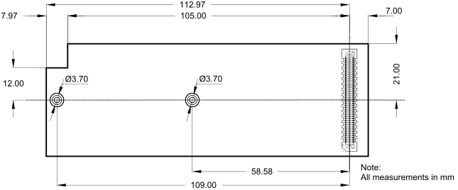
Fig. 2.8 Mezzanine board dimensions (bottom view)#