9. Hardware Guide#
This Hardware Guide provides information about the features, connectors and signals available on TIGER SOM-RK3588-Q7, as TIGER SOM-RK3588-Q7 has 2 different connectors; the main connection is Q7 and the sub connection is the FFC Connector, and so the FFC Connector will be discussed in related sections.
9.1. Q7 Implementation#
Q7 has mandatory and optional features. Following table shows the feature set of TIGER SOM-RK3588-Q7 compared to the minimum ARM/RISC based and maximum configuration according to the Q7 standard.
System I/O Interface |
Q7 Minimum |
RK3588_Q7 |
Q7 Maximum |
|---|---|---|---|
PCI Express lanes |
0 |
4 |
4 |
Serial ATA channels |
0 |
2 |
2 |
USB 2.0 ports |
1 |
1 |
8 |
USB 3.0 ports |
0 |
3 |
3 |
LVDS channels |
0 |
0 |
2 |
Embedded Display Port/ HDMI output |
0 |
1 |
1 |
MIPI_CSI |
0 |
1+(2 on FFC connectors) |
2 |
HDMI input |
0 |
(1 on FFC connectors) |
0 |
High Definition Audio / AC’97 / I2S |
0 |
1 |
1 |
Ethernet 10/100/1000 Mbps |
0 |
1x Gigabit |
1x Gigabit |
UART |
0 |
1+1 shared with GPIO |
1 |
GPIO |
0 |
8 |
8 |
Secure Digital I/O |
0 |
1 |
1 |
System Management Bus |
0 |
1 |
1 |
I²C Bus |
1 |
4 |
4 |
SPI Bus |
0 |
1 |
1 |
CAN Bus |
0 |
1 |
1 |
Watchdog Trigger |
1 |
1 |
1 |
Power Button |
1 |
1 |
1 |
Power Good |
1 |
1 |
1 |
Reset Button |
1 |
1 |
1 |
LID Button |
0 |
1 |
1 |
Sleep Button |
0 |
1 |
1 |
Suspend to RAM (S3 mode) |
0 |
1 |
1 |
Wake |
0 |
1 |
1 |
Battery low alarm |
0 |
1 |
1 |
Thermal control |
0 |
1 |
1 |
FAN control |
0 |
1 |
1 |
Note
TIGER SOM-RK3588-Q7 module is available in different variants. This document describes the maximum configuration. For details about orderable variants please refer to the order_code document.
Note
Not all interfaces are available at the same time as they might conflict with others.
9.2. Q7 Connector Pinout#
The following table shows the signals on the edge connector of the TIGER SOM-RK3588-Q7 module. Empty cells are simply not connected pins.
no. |
Q7 name |
CPU Pin name |
no. |
Q7 name |
CPU Pin name |
|---|---|---|---|---|---|
1 |
GND |
2 |
GND |
||
3 |
GBE_MDI3 |
(ETH PHY) |
4 |
GBE_MDI2 |
(ETH PHY) |
5 |
GBE_MDI3+ |
(ETH PHY) |
6 |
GBE_MDI2+ |
(ETH PHY) |
7 |
GBE_LINK100# |
(ETH PHY) |
8 |
GBE_LINK1000# |
(ETH PHY) |
9 |
GBE_MDI1 |
(ETH PHY) |
10 |
GBE_MDI0 |
(ETH PHY) |
11 |
GBE_MDI1+ |
(ETH PHY) |
12 |
GBE_MDI0+ |
(ETH PHY) |
13 |
GBE_LINK# |
(ETH PHY) |
14 |
GBE_ACT# |
(ETH PHY) |
15 |
GBE_CTREF |
16 |
SUS_S5# |
GPIO3_A5 |
|
17 |
WAKE# |
GPIO3_C6 |
18 |
SUS_S3# |
GPIO3_A6 |
19 |
GPO0 |
GPIO3_B0 |
20 |
PWRBTN# |
|
21 |
SLP_BTN#/ GPII1 |
GPIO4_B3 |
22 |
LID_BTN#/ GPII0 |
GPIO3_D4 |
23 |
GND |
24 |
GND |
||
25 |
GND |
26 |
PWGIN |
GPIO3_A0 |
|
27 |
BATLOW#/ GPII2 |
GPIO3_B5 |
28 |
RSTBTN# |
nPOR/ RESETB |
29 |
SATA0_TX+ |
Q7_PCIE20_0_TX/ SATA30_0_TX_P |
30 |
SATA1_TX+ |
Q7_PCIE20_1_TX/ SATA30_1_TX_P |
31 |
SATA0_TX |
Q7_PCIE20_0_TX/ SATA30_0_TX_N |
32 |
SATA1_TX |
Q7_PCIE20_1_TX/ SATA30_1_TX_N |
33 |
SATA_ACT# |
GPIO1_A1 |
34 |
GND |
|
35 |
SATA0_RX+ |
Q7_PCIE20_0_RX/ SATA30_0_RX_P |
36 |
SATA1_RX+ |
Q7_PCIE20_1_RX/ SATA30_1_RX_P |
37 |
SATA0_RX |
Q7_PCIE20_0_RX/ SATA30_0_RX_N |
38 |
SATA1_RX |
Q7_PCIE20_1_RX/ SATA30_1_RX_N |
39 |
GND |
40 |
GND |
||
41 |
BIOS_DISABLE#/ BOOT_ALT# |
SARA_IN0_BOOT |
42 |
SDIO_CLK# |
GPIO4_D5 |
43 |
SDIO_CD# |
GPIO0_A4 |
44 |
Reserved (was SDIO_LED) |
|
45 |
SDIO_CMD |
GPIO4_D4 |
46 |
SDIO_WP |
GPIO1_A4 |
47 |
SDIO_PWR# |
GPIO1_B4 |
48 |
SDIO_DAT1 |
GPIO4_D1 |
49 |
SDIO_DAT0 |
GPIO4_D0 |
50 |
SDIO_DAT3 |
GPIO4_D3 |
51 |
SDIO_DAT2 |
GPIO4_D2 |
52 |
Reserved (was SDIO_DAT5) |
|
53 |
Reserved (was SDIO_DAT4) |
54 |
Reserved (SDIO_DAT7) |
||
55 |
Reserved (was SDIO_DAT6) |
56 |
USB_OTG_PEN |
GPIO1_B5 |
|
57 |
GND |
58 |
GND |
||
59 |
HDA_SYNC/ I2S_WS |
GPIO3_A2 |
60 |
SMB_CLK/ GP1_I2C_CLK |
GPIO1_D6 |
61 |
HDA_RST#/ I2S_RST# |
GPIO1_A0 |
62 |
SMB_DAT/ GP1_I2C_DAT |
GPIO1_D7 |
63 |
HDA_BITCLK/ I2S_CLK |
GPIO3_A1 |
64 |
SMB_ALERT# |
GPIO3_C2 |
65 |
HDA_SDI/ I2S_SDI |
GPIO3_A4 |
66 |
GP0_I2C_CLK |
GPIO4_B6 |
67 |
HDA_SDO/ I2S_SDO |
GPIO3_A3 |
68 |
GP0_I2C_DAT |
GPIO4_B7 |
69 |
THRM# |
GPIO4_A1 |
70 |
WDTRIG# |
ATtiny pinPC2 |
71 |
THRMTRIP# |
GPIO4_A3 |
72 |
WDOUT |
ATtiny pinPB5 |
73 |
GND |
74 |
GND |
||
75 |
USB_P7/ USB_SSTX0 |
TYPEC1_SSTX1N/ DP1_TX1N |
76 |
USB_P6/ USB_SSRX0 |
TYPEC1_SSRX1N/ DP1_TX0N |
77 |
USB_P7+/ USB_SSTX0+ |
TYPEC1_SSTX1P/ DP1_TX1P |
78 |
USB_P6+/ USB_SSRX0+ |
TYPEC1_SSRX1P/ DP1_TX0P |
79 |
USB_6_7_OC# |
GPIO4_A6 |
80 |
USB_4_5_OC# |
GPIO4_A7 |
81 |
USB_P5/ USB_SSTX2 |
USB30_2_SSTXN |
82 |
USB_P4/ USB_SSRX2 |
USB30_2_SSRXN |
83 |
USB_P5+/ USB_SSTX2+ |
USB30_2_SSTXP |
84 |
USB_P4+/ USB_SSRX2+ |
USB30_2_SSRXP |
85 |
USB_2_3_OC# |
GPIO4_B0 |
86 |
USB_0_1_OC# |
GPIO4_A2 |
87 |
USB_P3 |
USB20_HOST1_DM |
88 |
USB_P2 |
USB20_HOST0_DM |
89 |
USB_P3+ |
USB20_HOST1_DP |
90 |
USB_P2+ |
USB20_HOST0_DP |
91 |
USB_VBUS |
USB_VBUSDET |
92 |
USB_ID |
TYPEC0_USB20_OTG_ID |
93 |
USB_P1 |
TYPEC0_USB20_OTG_DM |
94 |
USB_P0 |
TYPEC1_USB20_OTG_DM |
95 |
USB_P1+ |
TYPEC0_USB20_OTG_DP |
96 |
USB_P0+ |
TYPEC1_USB20_OTG_DP |
97 |
GND |
98 |
GND |
||
99 |
eDP0_TX0+/ LVDS_A0+ |
MIPI_DPHY0_TX_D0_P |
100 |
eDP1_TX0+/ LVDS_B0+ |
MIPI_CSI1_D0_P |
101 |
eDP0_TX0/ LVDS_A0 |
MIPI_DPHY0_TX_D0_N |
102 |
eDP1_TX0/ LVDS_B0 |
MIPI_CSI1_D0_N |
103 |
eDP0_TX1+/ LVDS_A1+ |
MIPI_DPHY0_TX_D1P |
104 |
eDP1_TX1+/ LVDS_B1+ |
MIPI_CSI1_D1P |
105 |
eDP0_TX1/ LVDS_A1 |
MIPI_DPHY0_TX_D1N |
106 |
eDP1_TX1/ LVDS_B1 |
MIPI_CSI1_D1N |
107 |
eDP0_TX2+/ LVDS_A2+ |
MIPI_DPHY0_TX_D2P |
108 |
eDP1_TX2+/ LVDS_B2+ |
MIPI_CSI1_D2P |
109 |
eDP0_TX2/ LVDS_A2 |
MIPI_DPHY0_TX_D2N |
110 |
eDP1_TX2/ LVDS_B2 |
MIPI_CSI1_D2N |
111 |
LVDS_PPEN |
GPIO3_C1 |
112 |
LVDS_BLEN |
GPIO3_C3 |
113 |
eDP0_TX3+/ LVDS_A3+ |
MIPI_DPHY0_TX_D3P |
114 |
eDP1_TX3+/ LVDS_B3+ |
MIPI_CSI1_D3P |
115 |
eDP0_TX3/ LVDS_A3 |
MIPI_DPHY0_TX_D3N |
116 |
eDP1_TX3/ LVDS_B3 |
MIPI_CSI1_D3N |
117 |
GND |
118 |
GND |
||
119 |
eDP0_AUX+/ LVDS_A_CLK+ |
MIPI_DPHY0_TX_CLKP |
120 |
eDP1_AUX+/ LVDS_B_CLK+ |
MIPI_CSI1_CLK0P |
121 |
eDP0_AUX/ LVDS_A_CLK |
MIPI_DPHY0_TX_CLKN |
122 |
eDP1_AUX/ LVDS_B_CLK |
MIPI_CSI1_CLK0N |
123 |
LVDS_BLT_CTRL/ GP_PWM_OUT0 |
GPIO1_D2 |
124 |
GP_1Wire_Bus/ HDMI_CEC |
GPIO0_C6 |
125 |
GP2_I2C_DAT/ LVDS_DID_DAT |
GPIO0_C7 |
126 |
eDP0_HPD#/ LVDS_BLC_DAT |
GPIO0_B6 |
127 |
GP2_I2C_CLK/ LVDS_DID_CLK |
GPIO0_D0 |
128 |
eDP1_HPD#/ LVDS_BLC_CLK |
GPIO0_B5 |
129 |
CAN0_TX |
GPIO0_B7 |
130 |
CAN0_RX |
GPIO0_C0 |
131 |
DP_LANE3+/ TMDS_CLK+ |
HDMI_TX0_D3P |
132 |
USB_SSTX1 |
TYPEC0_SSTX1N |
133 |
DP_LANE3/ TMDS_CLK |
HDMI_TX0_D3N |
134 |
USB_SSTX1+ |
TYPEC0_SSTX1P |
135 |
GND |
136 |
GND |
||
137 |
DP_LANE1+/ TMDS_LANE1+ |
HDMI_TX0_D1P |
138 |
DP_AUX+ |
EDP_TX0_AUXP |
139 |
DP_LANE1/ TMDS_LANE1 |
HDMI_TX0_D1N |
140 |
DP_AUX |
EDP_TX0_AUXN |
141 |
GND |
142 |
GND |
||
143 |
DP_LANE2+/ TMDS_LANE0+ |
HDMI_TX0_D0_P |
144 |
USB_SSRX1 |
TYPEC0_SSRX1N |
145 |
DP_LANE2/ TMDS_LANE0 |
HDMI_TX0_D0_N |
146 |
USB_SSRX1+ |
TYPEC0_SSRX1P |
147 |
GND |
148 |
GND |
||
149 |
DP_LANE0+/ TMDS_LANE2+ |
HDMI_TX0_D2P |
150 |
HDMI_CTRL_DAT |
GPIO0_D4 |
151 |
DP_LANE0/ TMDS_LANE2 |
HDMI_TX0_D2N |
152 |
HDMI_CTRL_CLK |
GPIO0_D5 |
153 |
DP_HDMI_HPD# |
GPIO1_A5 |
154 |
DP_HPD# |
GPIO4_B5 |
155 |
PCIE_CLK_REF+ |
156 |
PCIE_WAKE# |
GPIO4_A4 |
|
157 |
PCIE_CLK_REF |
158 |
PCIE_RST# |
GPIO3_B6 |
|
159 |
GND |
160 |
GND |
||
161 |
PCIE3_TX+ |
PCIE30_PORT1_TX1P |
162 |
PCIE3_RX+ |
PCIE30_PORT1_RX1P |
163 |
PCIE3_TX |
PCIE30_PORT1_TX1N |
164 |
PCIE3_RX |
PCIE30_PORT1_RX1N |
165 |
GND |
166 |
GND |
||
167 |
PCIE2_TX+ |
PCIE30_PORT1_TX0P |
168 |
PCIE2_RX+ |
PCIE30_PORT1_RX0P |
169 |
PCIE2_TX |
PCIE30_PORT1_TX0N |
170 |
PCIE2_RX |
PCIE30_PORT1_RX0N |
171 |
UART0_TX |
GPIO3_B1 |
172 |
UART0_RTS# |
GPIO3_B3 |
173 |
PCIE1_TX+ |
PCIE30_PORT0_TX1P |
174 |
PCIE1_RX+ |
PCIE30_PORT0_RX1P |
175 |
PCIE1_TX |
PCIE30_PORT0_TX1N |
176 |
PCIE1_RX |
PCIE30_PORT0_RX1N |
177 |
UART0_RX |
GPIO3_B2 |
178 |
UART0_CTS# |
GPIO3_B4 |
179 |
PCIE0_TX+ |
PCIE30_PORT0_TX0P |
180 |
PCIE0_RX+ |
PCIE30_PORT0_RX0P |
181 |
PCIE0_TX |
PCIE30_PORT0_TX0N |
182 |
PCIE0_RX |
PCIE30_PORT0_RX0N |
183 |
GND |
184 |
GND |
||
185 |
GPIO0 |
GPIO4_C0 |
186 |
GPIO1 |
GPIO4_A0 |
187 |
GPIO2 |
GPIO4_A5 |
188 |
GPIO3 |
GPIO3_B7 |
189 |
GPIO4 |
GPIO3_D0 |
190 |
GPIO5/ TSD_UART_TX |
GPIO3_C4 |
191 |
GPIO6/ TSD_UART_RX |
GPIO3_C5 |
192 |
GPIO7 |
GPIO1_B0 |
193 |
VCC_RTC |
194 |
SPKR/ GP_PWM_OUT2 |
ATtiny pin PB5 |
|
195 |
FAN_TACHOIN/ GP_TIMER_IN |
ATtiny pinPA6 |
196 |
FAN_PWMOUT/ GP_PWM_OUT1 |
ATtiny pin PA4 |
197 |
GND |
198 |
GND |
||
199 |
SPI_MOSI |
GPIO3_D2 |
200 |
SPI_CS0# |
GPIO4_B2 |
201 |
SPI_MISO |
GPIO3_D1 |
202 |
SPI_CS1# |
GPIO4_B1 |
203 |
SPI_SCK |
GPIO3_D3 |
204 |
MFG_NC4/ TRST |
|
205 |
VCC_5V_SB |
206 |
VCC_5V_SB |
||
207 |
MFG_NC0/ TCLK |
208 |
MFG_NC2/ TDI |
||
209 |
MFG_NC1/ TDO |
210 |
MFG_NC3/ TMS |
||
211 |
NC |
212 |
NC |
||
213 |
NC |
214 |
NC |
||
215 |
NC |
216 |
NC |
||
217 |
NC |
218 |
NC |
||
219 |
VCC |
220 |
VCC |
||
221 |
VCC |
222 |
VCC |
||
223 |
VCC |
224 |
VCC |
||
225 |
VCC |
226 |
VCC |
||
227 |
VCC |
228 |
VCC |
||
229 |
VCC |
VCC |
9.3. FFC Expansion Connector Pinout#
The following table shows the signals on the FFC connectors of the TIGER SOM-RK3588-Q7 module. Empty cells are simply not connected pins.
no. |
FFC Display-Name |
P2-(Top-FFC) Signal_Name |
P2-(Top-FFC) CPU_Pin/function |
P3-(bottom-FFC) Signal-Name |
P3-(bottom-FFC) CPU_Pin/function |
|---|---|---|---|---|---|
1 |
3V3 |
VCC3V3_S3 |
VCC3V3_S3 |
||
2 |
3V3 |
VCC3V3_S3 |
VCC3V3_S3 |
||
3 |
D0+ |
MIPI_CSI0_D0_P |
MIPI_CSI0_D0_P |
CSI2D0_P |
MIPI_DPHY0_RX_D0_P/ MIPI_CPHY0RX_TRIO0_B |
4 |
D0- |
MIPI_CSI0_D0_N |
MIPI_CSI0_D0_N |
CSI2D0_N |
MIPI_DPHY0_RX_D0_N/ MIPI_CPHY0RX_TRIO0_A |
5 |
GND |
GND |
GND |
||
6 |
D1+ |
MIPI_CSI0_D1_P |
MIPI_CSI0_D1P |
CSI2D1_P |
MIPI_DPHY0_RX_D1P/ MIPI_CPHY0RX_TRIO1_A |
7 |
D1 |
MIPI_CSI0_D1_N |
MIPI_CSI0_D1N |
CSI2D1_N |
MIPI_DPHY0_RX_D1N/ MIPI_CPHY0RX_TRIO0_C |
8 |
GND |
GND |
GND |
||
9 |
D2+ |
MIPI_CSI0_D2_P |
MIPI_CSI0_D2P |
||
10 |
D2 |
MIPI_CSI0_D2_N |
MIPI_CSI0_D2N |
||
11 |
RST# |
CSI0_RST |
GPIO0_B0 |
CSI2_RST |
SPI1CS1_M2/ PDM0SDI0_M0/ GPIO1_D5 |
12 |
D3+ |
MIPI_CSI0_D3_P |
MIPI_CSI0_D3P |
||
13 |
D3 |
MIPI_CSI0_D3_N |
MIPI_CSI0_D3N |
||
14 |
GND |
GND |
GND |
||
15 |
CLK+ |
MIPI_CSI0_CLK_P |
MIPI_CSI0_CLK0P |
CSI2C_P |
MIPI_DPHY0_RX_CLKP/ MIPI_CPHY0RX_TRIO1_C |
16 |
CLK |
MIPI_CSI0_CLK_N |
MIPI_CSI0_CLK0N |
CSI2C_N |
MIPI_DPHY0_RX_CLKN/ MIPI_CPHY0RX_TRIO1_B |
17 |
GND |
GND |
GND |
||
18 |
I2C_CLK |
I2C4_SCL_M4 |
I2C4_SCL_M4/ GPIO1_C7 |
I2C3_SCL_M0 |
I2C3_SCL_M0/ GPIO1_C1 |
19 |
I2C_DAT |
I2C4_SDA_M4 |
PWM15IR_M2/ I2C4_SDA_M4/ GPIO1_C6 |
I2C3_SDA_M0 |
I2C3_SDA_M0/ GPIO1_C0 |
20 |
ENA# |
CSI0_ENA |
GPIO2_B4 |
CSI2_ENA |
GPIO2_C5 |
21 |
MCLK |
CSI1/ 2_MCLK |
MIPI_CAMERA1_CLK_M0/ GPIO1_B6 |
CSI2/ 3_MCLK |
PWM13_M2/ MIPI_CAMERA2_CLK_M0/ GPIO1_B7 |
22 |
ENA# |
CSI1_ENA |
GPIO2_C4 |
HDMI_RX_HPDOUT_H |
HDMI_RX_HPDOUT_M1/ GPIO3_D4 |
23 |
I2C_CLK |
I2C2_SCL_M3 |
I2C2_SCL_M3/ GPIO1_C5 |
HDMIRX_D2P |
HDMIRX_D2P |
24 |
I2C_DAT |
I2C2_SDA_M3 |
PWM11IR_M2/ I2C2_SDA_M3/ GPIO1_C4 |
HDMIRX_D2N |
HDMIRX_D2N |
25 |
GND |
GND |
GND |
||
26 |
CLK+ |
CAM1CLK0_P |
MIPI_DPHY1_RX_CLKP/ MIPI_CPHY1RX_TRIO1_C |
HDMIRX_CLKP |
HDMIRX_CLKP |
27 |
CLK |
CAM1CLK0_N |
MIPI_DPHY1_RX_CLKN/ MIPI_CPHY1RX_TRIO1_B |
HDMIRX_CLKN |
HDMIRX_CLKN |
28 |
GND |
GND |
GND |
||
29 |
D0+ |
CAM1D0_P |
MIPI_DPHY1_RX_D0_P/ MIPI_CPHY1RX_TRIO0_B |
HDMIRX_D0_P |
HDMIRX_D0_P |
30 |
D0- |
CAM1D0_N |
MIPI_DPHY1_RX_D0_N/ MIPI_CPHY1RX_TRIO0_A |
HDMIRX_D0_N |
HDMIRX_D0_N |
31 |
RST# |
CSI1_RST |
GPIO4_C6 |
HDMI_RX_SDA_M0 |
HDMI_RX_SDA_M0/ GPIO0_D1 |
32 |
D1+ |
CAM1D1_P |
MIPI_DPHY1_RX_D1P/ MIPI_CPHY1RX_TRIO1_A |
HDMIRX_D1_P |
HDMIRX_D1P |
33 |
D1 |
CAM1D1_N |
MIPI_DPHY1_RX_D1N/ MIPI_CPHY1RX_TRIO0_C |
HDMIRX_D1_N |
HDMIRX_D1N |
34 |
GND |
GND |
GND |
||
35 |
CAM0_GPIO |
CSI0_GPIO0 |
GPIO2_B5 |
CSI2_GPIO0 |
SPI4MISO_M0/ UART3RX_M0/ I2C3_SDA_M0/ GPIO1_C0 |
36 |
CAM1_GPIO |
CSI1_GPIO1 |
GPIO0_B2 |
HDMI_RX_SCL_M0 |
HDMI_RX_SCL_M0/ GPIO0_D2 |
9.4. Signal Details#
9.4.1. Ethernet#
Q7 Signal |
Type |
Signal Level |
Description |
|---|---|---|---|
GBE_MDI[0:3]+ GBE_MDI[0:3]- |
I/O |
Analog |
Ethernet Controller: Media Dependent Interface Differential Pairs. The MDI can operate in 1000 and 100 Mbit/sec modes |
GBE_ACT# |
OC |
3.3V |
Ethernet Controller activity indicator, active low |
GBE_LINK# |
OC |
3.3V |
Ethernet Controller link indicator, active low |
GBE_LINK100# |
OC |
3.3V |
Internally connected to GBE_LINK# |
GBE_LINK1000# |
OC |
3.3V |
Internally connected to GBE_LINK# |
GBE_CTREF |
REF |
Analog |
Center Tap Voltage |
9.4.2. USB#
Q7 Signal |
Type |
Signal Level |
Description |
|---|---|---|---|
USB_P[0:4]+ USB_N[0:4]- |
I/O |
USB |
Hi-Speed USB differential pairs |
USB_SSTX_P[0:2]+ USB_SSTX_N[0:2]- |
I/O |
USB |
SuperSpeed USB differential transmit pairs |
USB_SSRX_P[0:2]+ USB_SSRX_N[0:2]- |
I/O |
USB |
SuperSpeed USB differential receive pairs |
USB_OC# |
I |
3.3V |
Over current detect input. The carrier board can signal an USB overcurrent condition pulling this pin low. |
USB_ID |
I |
3.3V |
Configures the mode of the USB Port 1. If the signal is an “active high” the Port will be configured as USB Client |
USB_VBUS |
I |
5.0V |
USB VBUS pin, 5V tolerant |
9.4.3. SDIO#
Q7 Signal |
Type |
Signal Level |
Description |
|---|---|---|---|
SDIO_CD# |
I |
3.3V |
SDIO Card Detect. This signal indicates when a SDIO/MMC card is present |
SDIO_CLK |
O |
3.3V |
SDIO Clock |
SDIO_CMD |
I/O |
3.3V |
SDIO Command/Response |
SDIO_WP |
I |
3.3V |
SDIO Write Protect |
SDIO_PWR# |
O |
3.3V |
SDIO Power Enable. This signal is used to enable the power being supplied to a SD/MMC card device |
SDIO_DAT0_3 |
I/O |
3.3V |
SDIO Data lines |
9.4.4. I2C#
Q7 Signal |
Type |
Signal Level |
Description |
|---|---|---|---|
Q7_I2C_CLK |
O |
3.3V |
I2C bus clock line connected to RK3588 |
Q7_I2C_DAT |
I/O |
3.3V |
I2C bus data line connected to RK3588 |
Q7_SMB_CLK |
O |
3.3V |
I2C bus clock line connected to RK3588 |
Q7_SMB_DAT |
I/O |
3.3V |
I2C bus data line connected to RK3588 |
Q7_HDMI_CTRL _CLK |
O |
3.3V |
I2C bus clock line connected to RK3588 |
Q7_HDMI_CTRL _DAT |
I/O |
3.3V |
I2C bus data line connected to RK3588 |
LVDS_DID_CLK /GP2_I2C_CLK |
O |
3.3V |
I2C bus clock line connected to RK3588, Secure Element, Attiny and Video connector |
LVDS_DID_DAT /GP2_I2C_DAT |
I/O |
3.3V |
I2C bus data line connected to RK3588, Secure Element, Attiny and Video connector |
LVDS_BLC_DAT |
O |
3.3V |
I2C bus clock line connected to RK3588, Video connector and carrier board EEPROM |
LVDS_BLC_CLK |
I/O |
3.3V |
I2C bus data line connected to RK3588, Video connector and carrier board EEPROM |
I2C signals on P2 (Top FFC)
Signal |
Type |
Signal Level |
Description |
|---|---|---|---|
I2C4_SCL_M4 |
O |
1.8V |
I2C bus 4 clock line connected to RK3588 |
I2C4_SDA_M4 |
I/O |
1.8V |
I2C bus 4 data line connected to RK3588 |
I2C2_SCL_M3 |
O |
1.8V |
I2C bus 2 clock line connected to RK3588 |
I2C2_SDA_M3 |
I/O |
1.8V |
I2C bus 2 data line connected to RK3588 |
I2C signals on P3 (Bottom FFC)
Signal |
Type |
Signal Level |
Description |
|---|---|---|---|
I2C3_SCL_M0 |
O |
1.8V |
I2C bus data line connected to RK3588_Q7 |
I2C3_SDA_M0 |
I/O |
1.8V |
I2C bus data line connected to RK3588_Q7 |
9.4.5. I2S#
Q7 Signal |
Type |
Signal Level |
Description |
|---|---|---|---|
Q7_I2S_RST |
O |
3.3V |
I2S Codec Reset |
Q7_I2S_SYNC |
O |
3.3V |
I2S Word select |
Q7_I2S_CLK |
O |
3.3V |
I2S Serial Data Clock |
Q7_I2S_SDO |
O |
3.3V |
I2S Serial Data Output |
Q7_I2S_SDI |
I |
3.3V |
I2S Serial Data Input |
9.4.6. Video#
TIGER SOM-RK3588-Q7 supports MIPI-DSI.
The MIPI_DSI specifications are:
MIPI DSI D_PHY v1.0
Up to four data lanes
Up to 1.0 Gbit/s per lane
The signal mapping is shown below:
Q7 Signal |
Function |
|---|---|
eDP0_TX0+/ LVDS_A0+ |
DSI_TX0+ |
eDP0_TX0/ LVDS_A0 |
DSI_TX0- |
eDP0_TX1+/ LVDS_A1+ |
DSI_TX1+ |
eDP0_TX1/ LVDS_A1 |
DSI_TX1- |
eDP0_TX2+/ LVDS_A2+ |
DSI_TX2+ |
eDP0_TX2/ LVDS_A2 |
DSI_TX2- |
eDP0_TX3+/ LVDS_A3+ |
DSI_TX3+ |
eDP0_TX3/ LVDS_A3 |
DSI_TX3- |
eDP0_AUX+/ LVDSA_CLK+ |
DSI_CLK+ |
eDP0_AUX/ LVDSA_CLK |
DSI_CLK- |
The TIGER SOM-RK3588-Q7 supports MIPI-CSI.
MIPI CSI D_PHY v1.0
Up to four data lanes
Up to 1.0 Gbps per lane
The signal function mapping for Q7 is shown below:
Q7 Signal |
Function |
|---|---|
eDP1_TX0+/ LVDS_B0+ |
CSI_D0+ |
eDP1_TX0/ LVDS_B0 |
CSI_D0- |
eDP1_TX1+/ LVDS_B1+ |
CSI_D1+ |
eDP1_TX1/ LVDS_B1 |
CSI_D1- |
eDP1_TX2+/ LVDS_B2+ |
CSI_D2+ |
eDP1_TX2/ LVDS_B2 |
CSI_D2- |
eDP1_TX3+/ LVDS_B3+ |
CSI_D3+ |
eDP1_TX3/ LVDS_B3 |
CSI_D3- |
eDP1_AUX+/ LVDSB_CLK+ |
CSI_CLK+ |
eDP1_AUX/ LVDSB_CLK |
CSI_CLK- |
9.4.7. CAN#
Q7 Signal |
Type |
Signal Level |
Description |
|---|---|---|---|
Q7_CAN0_TX |
O |
3.3V |
CAN TX output for CAN Bus channel 0 CPU pin GPIO0_B7 |
Q7_CAN0_RX |
I |
3.3V |
CAN RX input for CAN Bus channel 0 CPU pin GPIO0_C0 |
9.4.8. SPI#
Q7 Signal |
Type |
Signal Level |
Description |
|---|---|---|---|
Q7_SPI_MOSI |
O |
3.3V |
Master serial output/Slave serial input signal |
Q7_SPI_MISO |
I |
3.3V |
Master serial input/Slave serial output signal |
Q7_SPI_SCK |
O |
3.3V |
SPI clock output |
Q7_SPI_CS0# |
O |
3.3V |
SPI chip select 0 output |
Q7_SPI_CS1# |
O |
3.3V |
SPI chip select 1 output (used when two devices are connected) |
9.4.9. UART#
UART0, as specified in the Q7 standard, is implemented including hardware flow
control. This UART shows up in Linux as /dev/ttyS0.
Q7 Signal |
Type |
Signal Level |
Description |
|---|---|---|---|
Q7_UART0_TX |
O |
3.3V |
Serial data transmit |
Q7_UART0_RX |
I |
3.3V |
Serial data receive |
Q7_UART0_CTS# |
I |
3.3V |
Handshake signal: ready to send data |
Q7_UART0_RTS# |
O |
3.3V |
Handshake signal: ready to receive data |
A second UART, UART1, can be enabled on the GPIO pins. This UART shows up in Linux
as /dev/ttyS5.
Q7 Signal |
Alternate function |
Type |
Signal Level |
Description |
|---|---|---|---|---|
Q7_GPIO5 |
UART1_TX |
O |
3.3V |
Serial data transmit |
Q7_GPIO6 |
UART1_RX |
I |
3.3V |
Serial data receive |
the FFC connector is meant for use with cameras however its pins can also be used as an additional UART (not simultaneously): on FFC P2 (Top FFC Connector)
Signal |
Type |
Signal Level |
CPU/Linux Pin |
|---|---|---|---|
CSI0_ENA |
I |
1.8V |
UART7_RX_M0 |
CSI0_GPIO0 |
O |
1.8V |
UART7_TX_M0 |
9.4.10. Misc#
Signal |
Type |
Signal Level |
Description |
|---|---|---|---|
WDTRIG# |
I |
3.3V |
Watchdog trigger signal |
WDOUT |
O |
3.3V |
Watchdog event indicator |
SPKR |
O |
3.3V |
ATtiny pin PB5 used for external buzzer control |
BIOS_DISABLE# /BOOT_ALT# |
I |
3.3V |
Disables the onboard bootloader and uses the one the SD card instead. If no bootloader is available on the SD card it falls back to USB recovery mode |
THRMTRIP# |
O |
3.3V |
Thermal Trip indicates an overheating condition of the processor. If ‘THRMTRIP#’ goes active the system immediately transitions to the S5 State (Soft Off) |
FAN_PWMOUT /GP_PWM_OUT1 |
O |
3.3V |
PWM output for fan speed control. Alternate function general purpose PWM output. Function based on microcontroller firmware |
FAN_TACHOIN /GP_TIMER_IN |
I |
3.3V |
Fan tachometer input. Alternate function general purpose timer input. Function based on microcontroller firmware |
9.4.11. Power Management#
Signal |
Type |
Signal Level |
Description |
|---|---|---|---|
RSTBTN# |
I |
3.3V |
Reset button input. An active low signal resets the module |
BATLOW# |
I |
3.3V |
Battery low input |
WAKE# |
I |
3.3V |
External system wake event. An active low signal wakes the module from a sleep state |
SUS_S3# |
O |
3.3V |
Indicated that the system is in suspend to ram (S3) |
SUS_S5# |
O |
3.3V |
Indicated that the system is in soft_off state (S5) |
SLP_BTN# |
I |
3.3V |
Sleep button. Signals the system with an falling edge to transition into sleep or wake from a sleep state |
LID_BTN# |
I |
3.3V |
LID button. Low active signal to detect a LID switch to transition into sleep or wake from a sleep state |
9.4.12. Power#
Signal |
Nominal Input |
Description |
|---|---|---|
VCC |
5V |
Main supply for the module |
VCC_RTC |
3V |
Backup supply for the RTC. If not used it can be left unconnected. Typical current: 1.4uA |
9.5. On-board Devices#
9.5.1. RAM#
Up to 32 GB RAM of LPDDR4X RAM
9.5.2. eMMC#
Up to 128GB eMMC connected through the 8-bit wide SDIO interface on the CPU.
Signal |
CPU Pin |
Linux GPIO # |
|---|---|---|
RESET |
GPIO2_A3 |
67 |
9.5.3. Companion Controller#
An On_board microcontroller provides additional features to the CPU. The controller is an ATtiny exposed via I2C and UPDI lines (pins UART4_TX_M2/GPIO_1_B3, UART4_RX_M2/GPIO_1_B2). As for the first controller, it emulates standard ICs and does not need custom drivers in Linux.
Feature |
CPU Connection |
Emulated IC |
Qseven Pins |
|---|---|---|---|
RTC |
I2C |
ISL1208 |
none |
Temperature sensor and fan controller |
I2C |
AMC6821 |
FAN_TACHOIN, FAN_PWMOUT |
Note
Please refer to Section 7 Companion controller features for instructions on how to flash Mule ATtiny.
9.5.4. Ethernet PHY#
The Texas Instruments DP83825IRMQR is connected to the CPU via RGMII and MDIO. Further connections are shown below.
PHY signal |
Connected to |
|---|---|
RESET |
CPU pin GPIO4_C3 |
MDIO |
CPU pin GPIO4_C5 |
MDC |
CPU pin GPIO4_C4 |
LED1 |
Qseven GBE_LINK1000 and GBE_LINK100 and GBE_LINK (tied together) |
LED2 |
Qseven GBE_ACT |
9.5.5. Test points TIGER SOM-RK3588-Q7#
Test point |
Connected to |
|---|---|
TP1 |
VCCA_1V8_S0 |
TP2 |
VDD_DDR_S0 |
TP3 |
VDD_GPU_S0 |
TP4 |
VCC_1V8_S0 |
TP5 |
VDDA_1V2_S0 |
TP6 |
VCCA_3V3_S0 |
TP7 |
VCCIO_SD_S0 |
TP8 |
VDD2_DDR_S3 |
TP9 |
VDD_CPU_LIT_S0 |
TP10 |
VDD_0V75_S3 |
TP11 |
VDDA_DDR_PLL_S0 |
TP12 |
VDDA_0V75_S0 |
TP13 |
VDDA_0V85_S0 |
TP14 |
VDD_0V75_S0 |
TP15 |
VDDQ_DDR_S0 |
TP16 |
VDD_LOG_S0 |
TP17 |
VCC_3V3_S3 |
TP18 |
VDD_VDENC_S0 |
TP19 |
VCC_1V8_S3 |
TP20 |
VCC_2V0_PLDO_S3 |
TP21 |
VDD_CPU_BIG0_S0 |
TP22 |
VDD_CPU_BIG1_S0 |
TP23 |
VDD_NPU_S0 |
TP24 |
VCC_1V1_NLDO_S3 |
TP25 |
VCC_1V2_S3 |
TP26 |
VDC |
TP27 |
ETH_TXC |
TP28 |
ATtiny DEBUG-RX |
TP29 |
ATtiny DEBUG-TX |
9.6. Using GPIOs#
Many Qseven signals can be reused as a general purpose I/O pin. The following table shows the mapping of the Q7 pins to CPU Pin and Linux GPIO number.
All listed pins are bidirectional when configured as GPIO.
Q7 Pin |
Signal |
CPU Pin |
Linux# |
|---|---|---|---|
16 |
SUS_S5# |
GPIO3_A5 |
101 |
17 |
WAKE# |
GPIO3_C6 |
118 |
18 |
SUS_S3# |
GPIO3_A6 |
102 |
19 |
GPiO0 |
GPIO3_B0 |
104 |
21 |
SLP_BTN# |
GPIO4_B3 |
139 |
22 |
LID_BTN# |
GPIO3_D5 |
125 |
26 |
Q7_PWGIN |
GPIO3_A0 |
96 |
27 |
BATLOW# |
GPIO3_B5 |
109 |
42 |
SDIO_CLK# |
GPIO4_D5 |
157 |
43 |
SDIO_CD# |
GPIO0_A4 |
4 |
45 |
SDIO_CMD |
GPIO4_D4 |
156 |
46 |
SDIO_WP |
GPIO1_A4 |
36 |
47 |
SDIO_PWR# |
GPIO1_B4 |
44 |
48 |
SDIO_DAT1 |
GPIO4_D1 |
153 |
49 |
SDIO_DAT0 |
GPIO4_D0 |
152 |
50 |
SDIO_DAT3 |
GPIO4_D3 |
155 |
51 |
SDIO_DAT2 |
GPIO4_D2 |
154 |
56 |
USB_DRIVE_BUS |
GPIO1_B5 |
45 |
59 |
I2S_WS |
GPIO3_A2 |
98 |
60 |
SMB_CLK |
GPIO1_D6 |
62 |
61 |
I2S_RST |
GPIO1_A0 |
32 |
62 |
SMB_DAT |
GPIO1_D7 |
63 |
63 |
I2S_CLK |
GPIO3_A1 |
97 |
64 |
SMB_ALERT |
GPIO3_C2 |
114 |
65 |
I2S_SDI |
GPIO3_A4 |
100 |
66 |
I2C_CLK |
GPIO4_B6 |
142 |
67 |
I2S_SDO |
GPIO3_A3 |
99 |
68 |
GP0_I2C_DAT |
GPIO4_B7 |
143 |
69 |
THRM |
GPIO4_A1 |
129 |
71 |
THRMTRIP# |
GPIO4_A3 |
131 |
79 |
USB_6_7_OC |
GPIO4_A6 |
134 |
80 |
USB_4_5_OC |
GPIO4_A7 |
135 |
85 |
USB_2_3_OC |
GPIO4_B0 |
136 |
86 |
USB_0_1_OC |
GPIO4_A2 |
130 |
111 |
eDP_PPEN |
GPIO3_C1 |
113 |
112 |
eDP_BLEN |
GPIO3_C3 |
115 |
123 |
eDP_BLT_CTRL GP_PWM_OUT0 |
GPIO1_D2 |
58 |
125 |
LVDS_DID_DAT |
GPIO0_C7 |
23 |
126 |
LVDS_BLC_DAT |
GPIO0_B6 |
14 |
127 |
LVDS_DID_CLK |
GPIO0_D0 |
24 |
128 |
LVDS_BLC_CLK |
GPIO0_B5 |
13 |
129 |
CAN0_TX |
GPIO0_B7 |
15 |
130 |
CAN0_RX |
GPIO0_C0 |
16 |
150 |
HDMI_CTRL_DAT |
GPIO0_D4 |
28 |
152 |
HDMI_CTRL_CLK |
GPIO0_D5 |
29 |
153 |
153_HDMI_HPD# |
GPIO1_A5 |
37 |
154 |
DP_HPD# |
GPIO4_B5 |
141 |
156 |
Q7_PCIE_WAKE# |
GPIO4_A4 |
132 |
158 |
Q7_PCIE_RST# |
GPIO3_B6 |
110 |
171 |
UART0_TX |
GPIO3_B1 |
105 |
172 |
UART0_RTS# |
GPIO3_B3 |
107 |
177 |
UART0_RX |
GPIO3_B2 |
106 |
178 |
UART0_CTS# |
GPIO3_B4 |
108 |
185 |
GPIO0 |
GPIO4_C0 |
144 |
186 |
GPIO1 |
GPIO4_A0 |
128 |
187 |
GPIO2 |
GPIO4_A5 |
133 |
188 |
GPIO3 |
GPIO3_B7 |
111 |
189 |
GPIO4 |
GPIO3_D0 |
120 |
190 |
GPIO5 |
GPIO3_C4 |
116 |
191 |
GPIO6 |
GPIO3_C5 |
117 |
192 |
GPIO7 |
GPIO1_B0 |
40 |
199 |
SPI_MOSI |
GPIO3_D2 |
122 |
200 |
SPI_CS0# |
GPIO4_B2 |
138 |
201 |
SPI_MISO |
GPIO3_D1 |
121 |
202 |
SPI_CS1# |
GPIO4_B1 |
137 |
203 |
SPI_SCK |
GPIO3_D3 |
123 |
The FFC expansion connectors are meant for use with cameras however it’s pins can also be used as GPIOs:
P3 (Bottom FFC connector):
Signal |
Type |
Signal Level |
CPU Pin |
Linux GPIO# |
|---|---|---|---|---|
I2C3_SCL_M0 |
I/O |
1.8V |
GPIO1_C1 |
49 |
I2C3_SDA_M0 |
I/O |
1.8V |
GPIO1_C0 |
48 |
CSI2_RST |
I/O |
1.8V |
GPIO1_D5 |
61 |
CSI2_ENA |
I/O |
1.8V |
GPIO2_C5 |
85 |
CSI2/3_MCLK |
I/O |
1.8V |
GPIO1_B7 |
47 |
HDMI_RX_HPD |
I/O |
3.3V |
GPIO3_D4 |
124 |
HDMI_RX_SDA |
I/O |
3.3V |
GPIO0_D1 |
25 |
HDMI_RX_SCL |
I/O |
3.3V |
GPIO0_D2 |
26 |
CSI2_GPIO0 |
I/O |
1.8V |
GPIO0_A0 |
0 |
P2 (Top FFC connector):
Signal |
Type |
Signal Level |
CPU Pin |
Linux GPIO# |
|---|---|---|---|---|
I2C4_SCL_M4 |
I/O |
1.8V |
GPIO1_C7 |
55 |
I2C4_SDA_M4 |
I/O |
1.8V |
GPIO1_C6 |
54 |
CSI0_ENA |
I/O |
1.8V |
GPIO2_B4 |
76 |
CSI1/ 2_MCLK |
I/O |
1.8V |
GPIO1_B6 |
46 |
CSI1_ENA |
I/O |
1.8V |
GPIO2_C4 |
84 |
CSI0_GPIO0 |
I/O |
1.8V |
GPIO2_B5 |
77 |
CSI1_GPIO1 |
I/O |
1.8V |
GPIO0_B2 |
10 |
I2C2_SCL_M3 |
I/O |
1.8V |
GPIO1_C5 |
53 |
I2C2_SDA_M3 |
I/O |
1.8V |
GPIO1_C4 |
52 |
To calculate the Linux GPIO # for CPU pins, use the following formula:
n = (block_number * 32) + (sub_block_number * 8) + index
Where:
block_number… index of the block numbersub_block_number… the alphabetical index of the block name, minus 1index… the pin number within the block
Example:
GPIO3_C6 -> (3 * 32) + (2 * 8) + 6 = 118
To enable a GPIO, write the Linux GPIO # to the special export file:
$ echo 118 > /sys/class/gpio/export
$ cat /sys/class/gpio/gpio118/direction
in
$ cat /sys/class/gpio/gpio118/value
0
To set the direction to output, write out in the GPIO’s direction file:
echo out > /sys/class/gpio/gpio118/direction
echo 1 > /sys/class/gpio/gpio118/value
The GPIO will be set to a value of 1 (high at 3.3V).
9.7. Electrical Specification#
9.7.1. Power Supply#
The power supply requirements are listed in the table below and are identical to the Qseven specification.
Rail |
Description |
Nominal voltage |
Tolerance |
|---|---|---|---|
VCC |
Main power supply |
5V |
4.75 … 5.25V |
VCC_RTC |
Backup battery |
3V |
2.4 … 3.3V |
9.8. Mechanical Specification#
9.8.1. Module Dimensions#
The mechanical dimensions of the module are shown below.
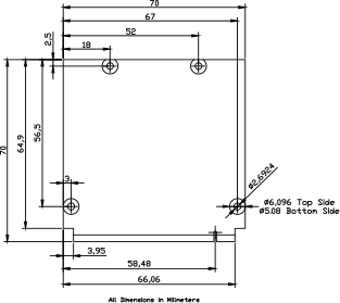
Fig. 9.1 Module dimensions (all values in mm)#
9.8.2. HAIKOU CB-MINI-ITX Dimension#
The mechanical dimensions of HAIKOU CB-MINI-ITX match the Mini-ITX form factor and can be mounted in a standard Mini-ITX PC Case.